Introduction
Hidden Markov Model (HMM) is a well established mathematical model for signal processing. It is used mainly in speech processing but it has also a wide range of application in different domains.
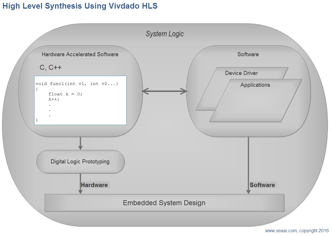
In this tutorial we will present a simple prototype for a single HMM using Vivado HLS. We will also explain how to drive the development chain from C language high level down to embedded system design using Xilinx Vivado and Vivado SDK.
IMPORTANT: HMM implementation in this document is meant only for educational purposes. If you are looking for actual HMM solution, SEAAI do provides more elaborated highly optimized solutions.
Vivado HLS allows you to use high level programming language like C or C++ to develop a hardware prototype. This brings great advantage to the development process by allowing the use
of the same programming language for Software and Hardware development.
HMM Prototyping In C
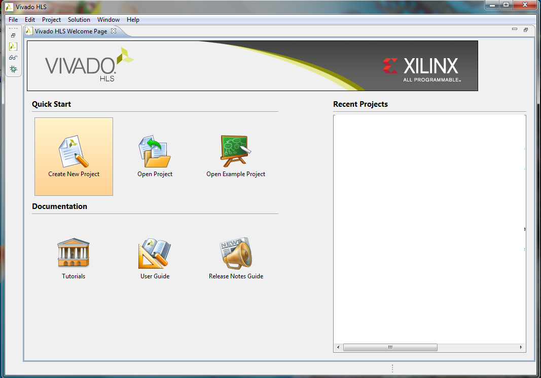
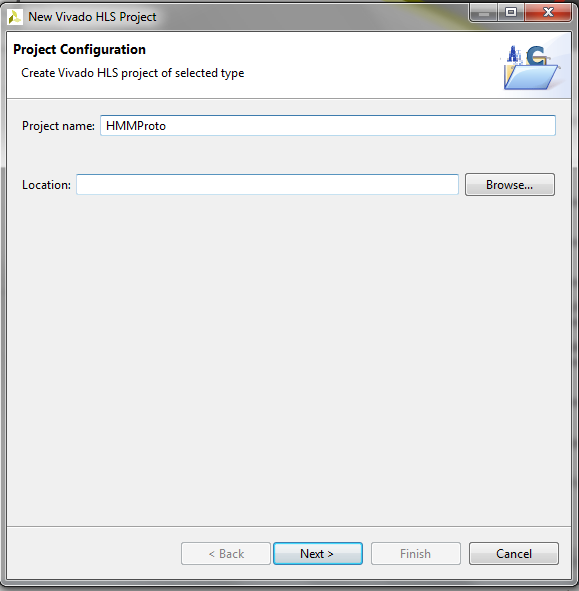
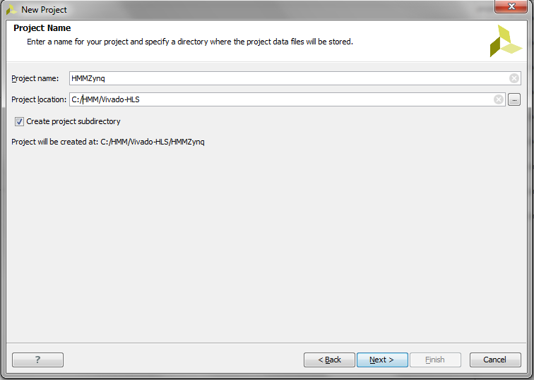
To start creating our HMM prototype we will create a new Vivado HLS project. Start Vivado HLS then click on New Project.
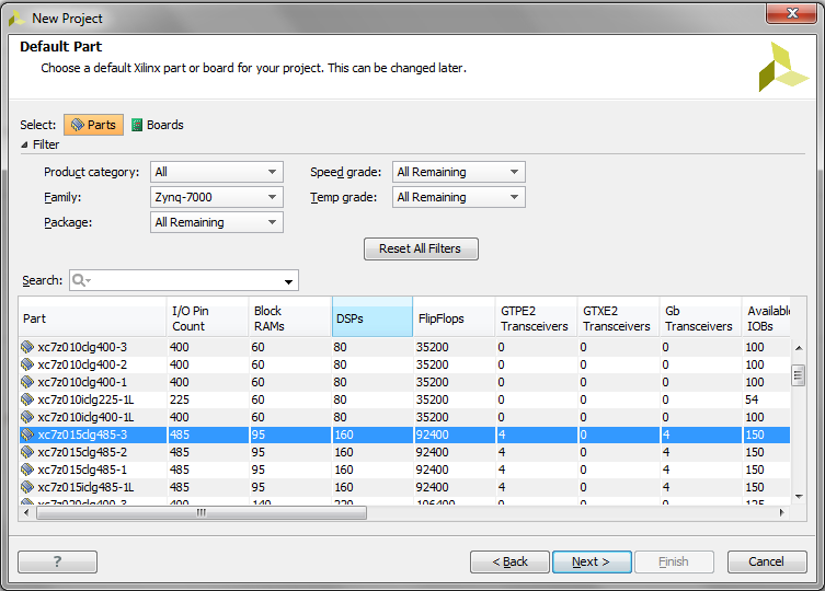
In this tutorial we have selected Zynq family part xc7z030isbv485-2l. In case your intention is to use different FPGA then it is better to specify the part that you are using. In what follows we will show how to build the embedded solution using
Zynq SoC. If you do not have a Zynq board then you can
specify your own Device/Board in here then build your own solution later, in
Vivado, using MicroBlaze processor wizard.

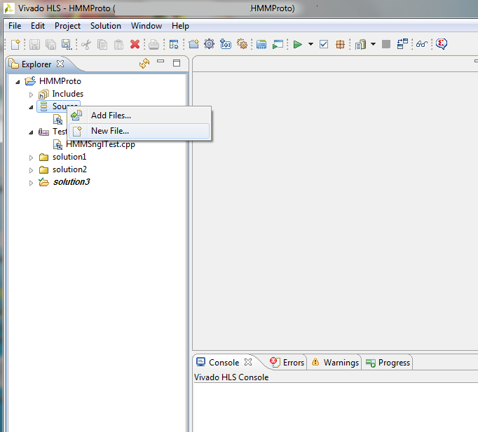
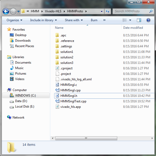
Copy source files "HMMSngl.cpp", "HMMSnglTest.cpp" to your project directory, or create new source then Copy-Past the source code inside the file.
You can download source files at this link. Make sure that "HMMSngl.cpp" is under Source and "HMMSnglTest.cpp" is under Test Bench. HMMSngl.cpp contains the actual function to prototype over FPGA.
HMMSnglTest.cpp and any other files under Test Bench are used to provide high level (C language level) and low level (VHDL/RTL simulation) to test your prototype functions.
For include file, you have to copy it or
create it outside Vivado. Simply copy include file "HMMSngl.h" to your project
directory.
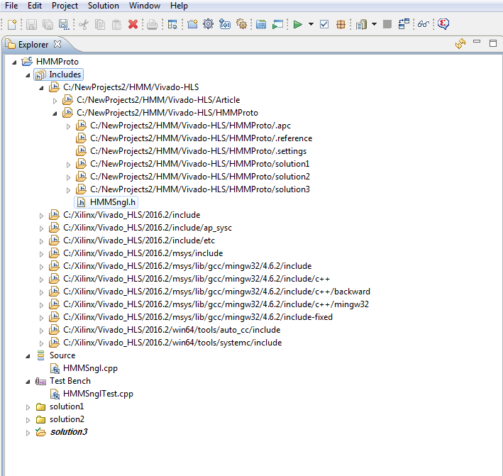
To make sure that include file is correctly referenced inside Vivado HLS, open Includes in Explorer Tab.
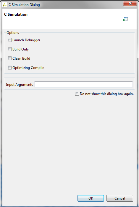
First step to validate your project is to try to compile it using C compiler. Select Project->Run C Simulation. Here is explanation of C Simulation
Dialog options:
-
Lunch Debugger: will start the C debugger and halt execution at the start of the Test Bench source.
-
Build only: will only compile and build your project in C.
If Build only is not selected then C simulation will be performed by executing all
the code in Test Bench file "MMSnglTest.cpp".
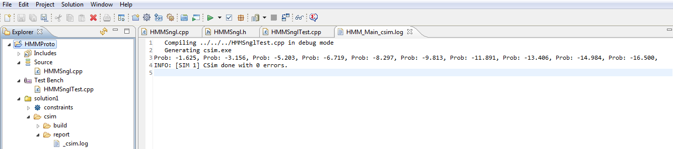
When you select to perform C Simulation, Vivado HLS will create automatically a solution -Solution1- for your project. Inside this solution directory you can find that Vivado HLS
did generate an executable file csim.exe.
You should be able to see the output generated by HMMSnglTest.cpp displayed in
the .log file. Vivado HLS project development cycle is organized in solutions.
Each solution will contains C Simulation, Synthesis, RTL Simulation and
Implementation output (code, reports, binaries etc..). The reason why you need
multiple solutions is that as a developer you will be trying different
optimization and interfacing directives on C, or *.CPP file level. For each
solution, you can define different directives. Some of the directives are in
charge of defining the Interface of your prototype and others are for
providing instruction on how to implement and optimize high level C code into low level
logic gates.
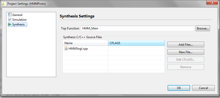
Before going into Synthesis, we need to specify the top function in our design.
This is necessary, so that RTL Synthesis is capable of knowing the IN/OUT design function.
Select Project->Settings, then click on the Synthesis Tab. Click on Browse and select the function HMM_Main
Select Solution->Run C Synthesis->Active Solution to start the synthesis of Solution1.
The Synthesis operation will transfer the combination of your source code and your directives into low level RTL design.
It is important to underline that the design generated by the Synthesis operation is oriented to the device or board that you have defined at the start.
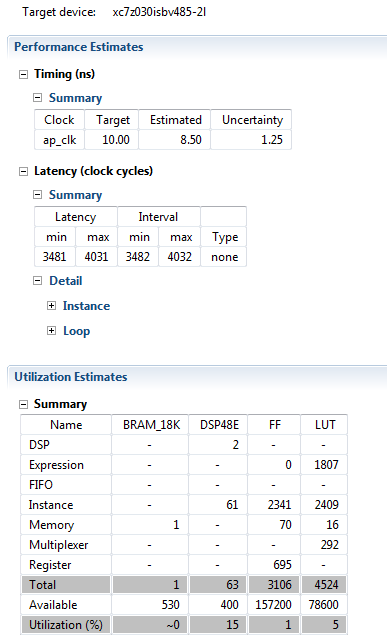
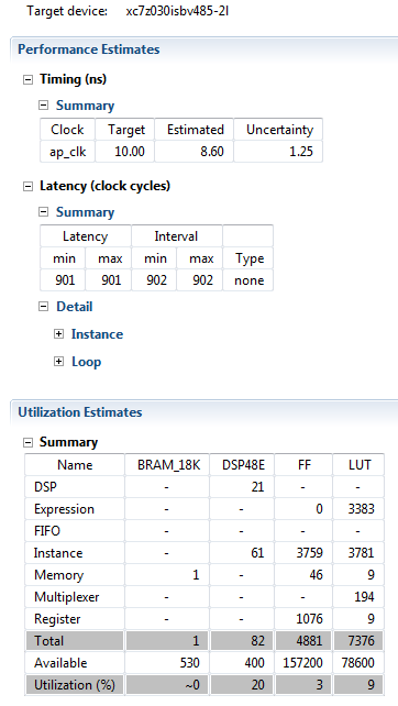
When the Synthesis operation is completed, Synthesis Report will be displayed. In Synthesis Report you can examine the results under three catgeories:
-
Performance Estimate: Provides an estimation of the run-time required by the prototype to perform required operations.
In our example we can read that the clock is defined at 10 ns period. Under Latency, we can read the Latency values.
Latency is the most important value about synthesis performance. It represents execution time in clock period time unit.
We can read for Solution1 that max Latency is 4031 which means 4031*CLock_Period
= 40310 ns
-
Utilization Estimates: Shows the utilization plan of the resources on the FPGA
device.
-
Interface: explains the assigned input/output pins of the your prototype.
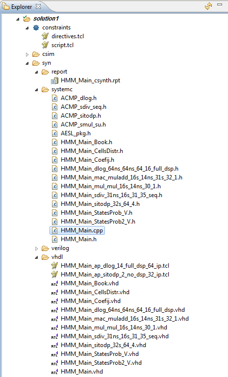
As a result for the synthesis, lower level source code, is generated for vhdl, verilog and SystemC programming languages. You can examine these files under Solution\Syn directory.
You can actually use any of automatically generated files to further develop your prototype using a specific language. Vivado HLS uses these sources during Post-Synthesis RTL Simulation.
RTL Simulation is not covered in this tutorial.
To start analyzing what was produced by the Synthesis, we will switch to Analysis view in Vivado HLS. For that, click on Analysis Button
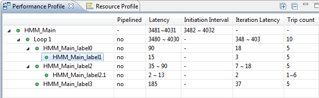
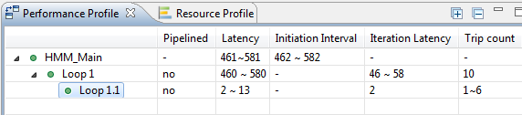
In Performance Profile, expand the the nested loops tree to be able to examine time performance
for each loop. For each row, Iteration Latency displays one pass loop run time cost in clock period time unit
and Trip Count displays how many times the loop is executed. For example,
each iteration of HMM_Main_lable1 costs 3 cycles that are repeated 5 times which
result in 15 cycle latency.
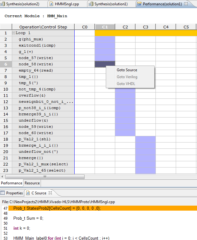
To the right, a listing of the sub "operations" executed inside each loop. A very useful feature is the ability to navigate directly to the source code. You can click on the cell then right click and select Goto Source.
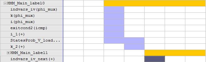
To further understand latency values shown in Performance Profile, let us
examine the latency necessary for HMM_Main_label0 (Markov Transition) loop. Even
that the inner loop costs 15 cycles only, the outer loop costs 18 cycles. We can
investigate this by examining
performance details in the right panel. We can see that HMM_Main_label1 takes 3
cycles. For 5 Iterations, 15 cycles are consumed by HMM_Main_label1. By
examining the detailed operations diagram we see that there are 2 cycles used by
HMM_Main_label0 in preparation for loop HMM_Main_label1. Those are
StatesProb_V_Load and k_2. This sums up to 17 cyles. Also, after inner loop
HMM_Main_label1's completion there is an extra cycle indvars_iv_next(+) that add 1
more cycle which makes the total count 18 cycles.
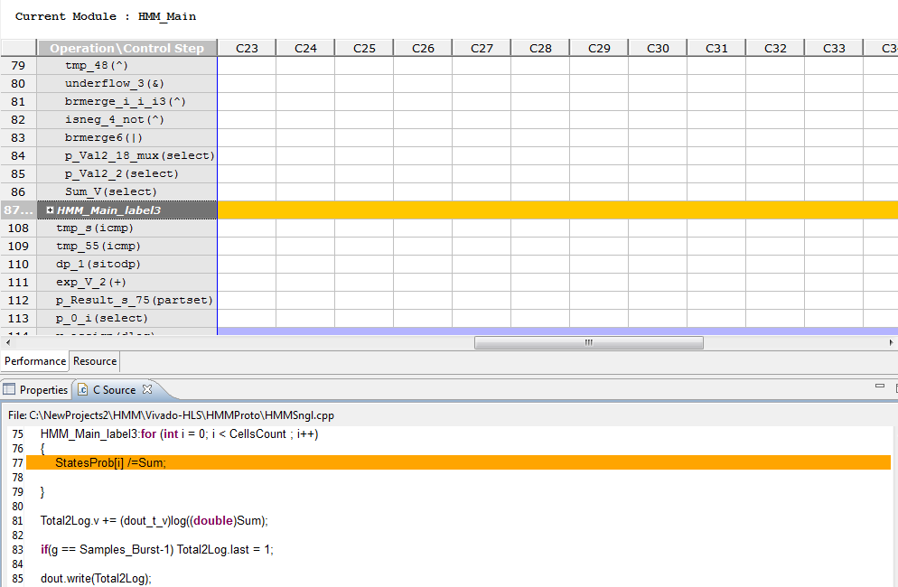
To investigate more reasons for solution latency, let us examine HMM_Main_label3
execution. We see that it is taking relatively considerable time corresponding
to the normalization step in source code line 77. This is also the case for
steps necessary for operations at source line 81.
Next, we will concentrate on enhancing the performance by adding directives to
optimize transition loop HMM_Main_label0 and HMM_Main_label1. For that, we start
by creating a new solution Solution2. Select menu item Project->New Solution
to create solution3. To add directives, follow these steps:
-
Open the source files
-
Select menu item Window->Show View->Directives.
-
Click in the Directives window to select the element for which you want to add a directive.
-
Right click the element and select Insert Directive
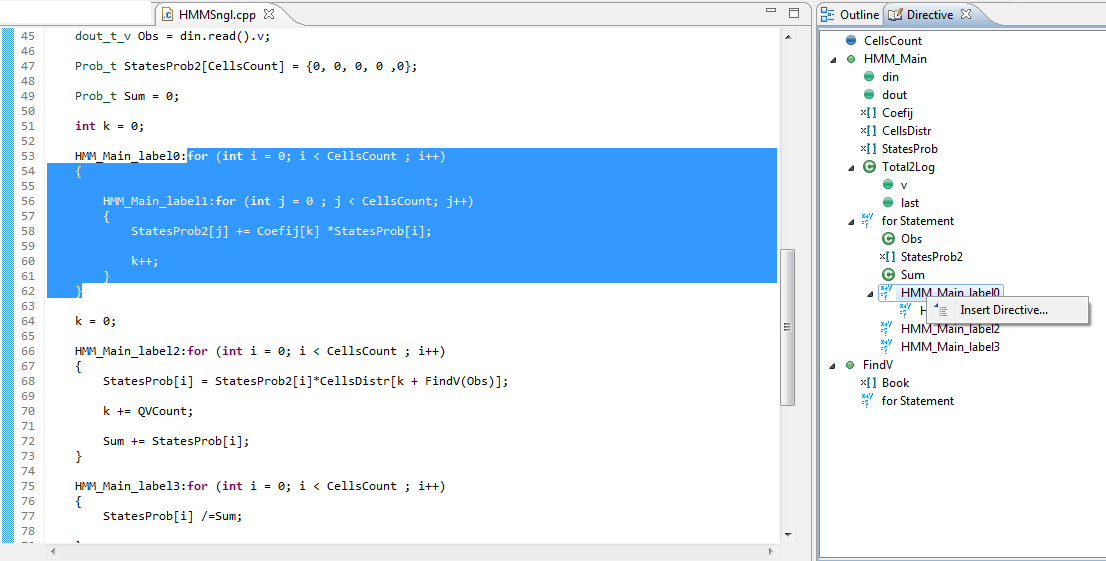
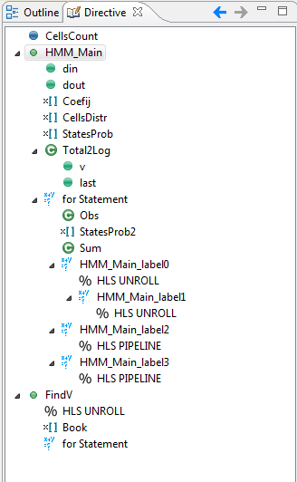
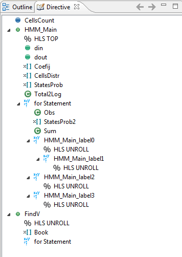
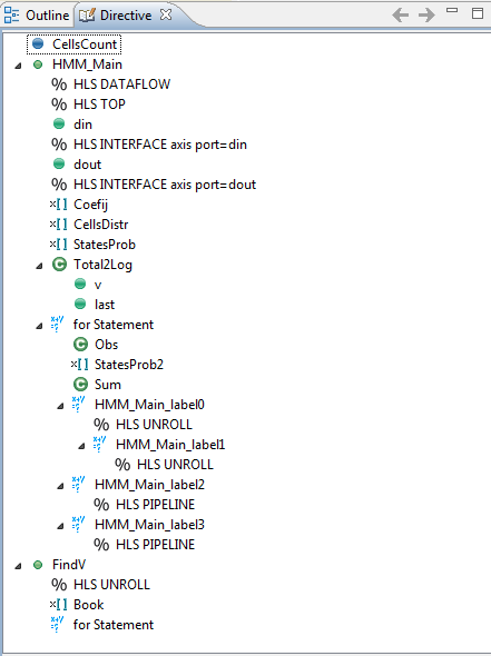
For solution2, we will add the directives HLS_UNROLL for HMM_Main_label0, HMM_Main_label1
and
FindV. Also, we will add HLS_PIPELINE for HMM_Main_label2 and HMM_Main_label3.
HLS_UNROLL instructs Vivado HLS to flatten the loop into direct distinct parallel operations executed at once.
HLS_PIPELINE instructs Vivado HLS to enhance loop execution by early data access and early result calculation. It is necessary to understand that a directive is not always applicable.
You can insert a directive but Vivado HLS will optimize the design according to your directive only if the code allows it.
Directives for Solution2 are displayed in the screenshot below.
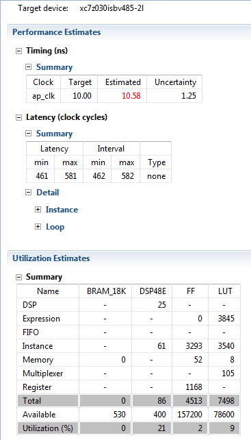
After inserting the directive, select Solution->Run C Synthesis->Active Solution to perform the synthesis of the new solution. After Synthesis, you can observe that performance was enhanced greatly by
the fact that latency
equals now to 902. In comparision with solution1's latency (4032), this represents
more than 4 times speed enhancement.
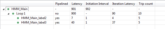
By examining the Performance report, we see that HMM_Main_label0 and HMM_Main_label1 were actually merged into direct operations that do not take more than
6 cycles. The remaining of the latency is consumed by HMM_Main_label2 and HMM_Main_label3. Concerning HMM_Main_label2,
pipelining was successful and we can observe that operations for source line 68 were executed in 4 cycles only.
Also, HMM_Main_label3 pipeline directive was successful in reducing required cycles times.
The resulting Latency is 90 cycles because. It is not easy to show how to
understand the calculation of this value because it is the result of pipelining
multiple iterative steps. But we can mention that Sum needs to be calculated completely before applying the normalization.
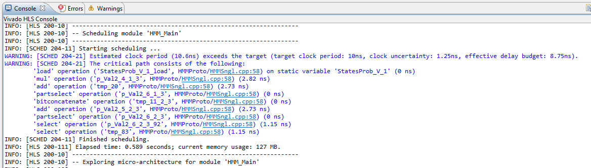
One can always take a look to the console output to get a precise idea of which of the directives
was actually performed by Vivado HLS.
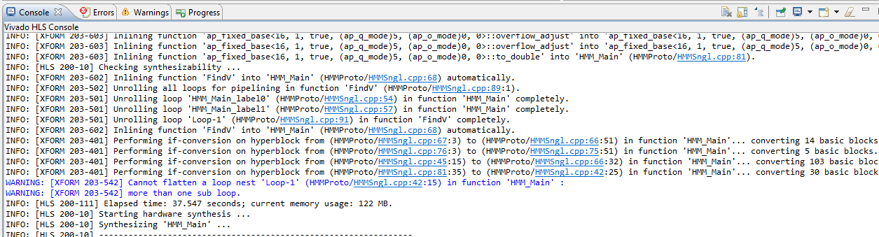
Next we will try more optimization in a new solution. Do as previous and create a new solution -Solution3. Open the source file HMMSngl.cpp and insert the directives as in the screenshot below
After inserting the directive, select Solution->Run C Synthesis->Active Solution to perform the synthesis of the new solution. After Synthesis, you can observe that performance was enhanced down to 581 cycles.
Also, you can see that Estimated clock delay is displayed in red which means that there may be flaws in the design due to signal propagation delay.
Potential design flows are actually detailed in the Synthesis console output.
You can examine Performance report and see that all loops were totally flattened with single remaining top loop.
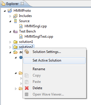
For this tutorial we will select solution2 since it did not present any warnings. Select Solution3 in explorer and right click to set it as active.
Before going further we need to setup our prototype interfaces. An Interface defines the way data are presented and pulled out to/from the system.
In any practical development, you have to define interfaces to connect your prototype to other equipment like
a processor, memory controller, etc..
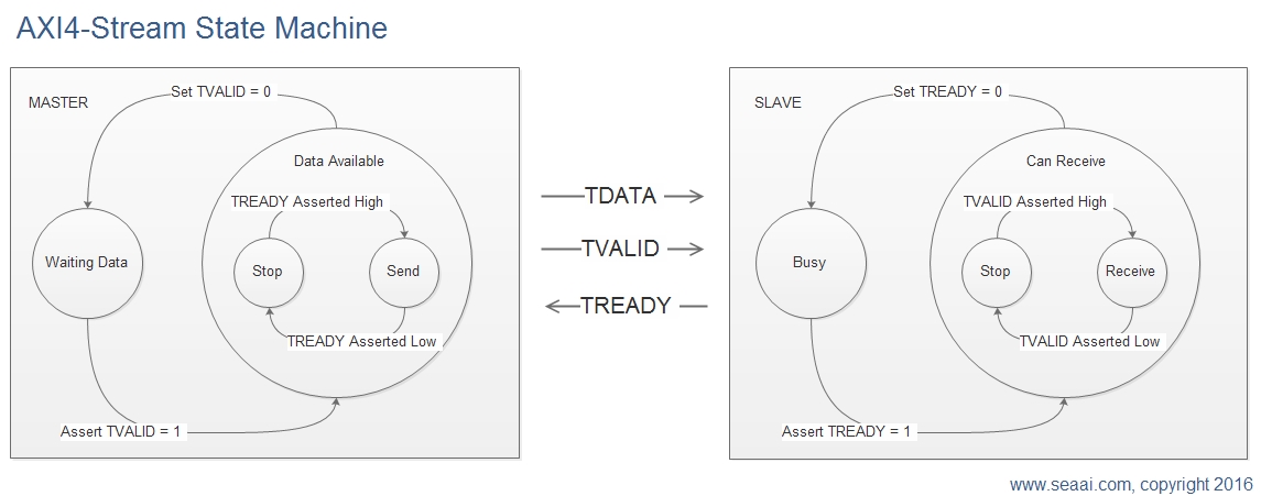
Because we are using DMA access, AXI4-Stream Bus interface is an ideal choice. AXI4-Stream basic signals are TREADY, TVALID and TDATA. TREADY informs the master that the salve is ready for data transfer. TVALID informs the slave that TDATA contains valid data to be received by the slave. Below is a simple state machine diagram for AXi4-Stream interface.
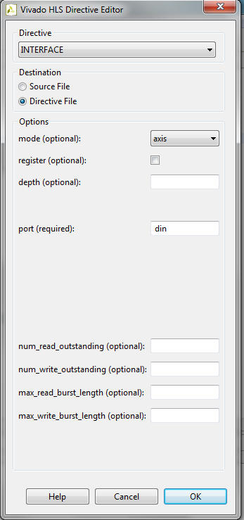
For our prototype, insert the following directives:
- Directive HLS_DATAFLOW for the main function
- Directive HLS_TOP for the main function
- HLS_INTERFACE axis for din variable
- HLS_INTERFACE axis for the dout variable
HLS_INTERFACE axis directive defines AXI4-Stream bus architecture for the input/output variable.
To finalize our work in creating the IP, select menu item Solution->Export RTL. Disable Evaluate checkbox, select IP Catalog and click Ok
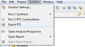
This will create the final IP package for your solution under the directory imp\IP. Actually, all files and information concerning your design IP are contained in the *.zip file.
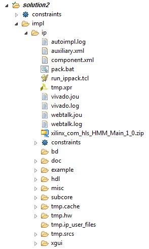
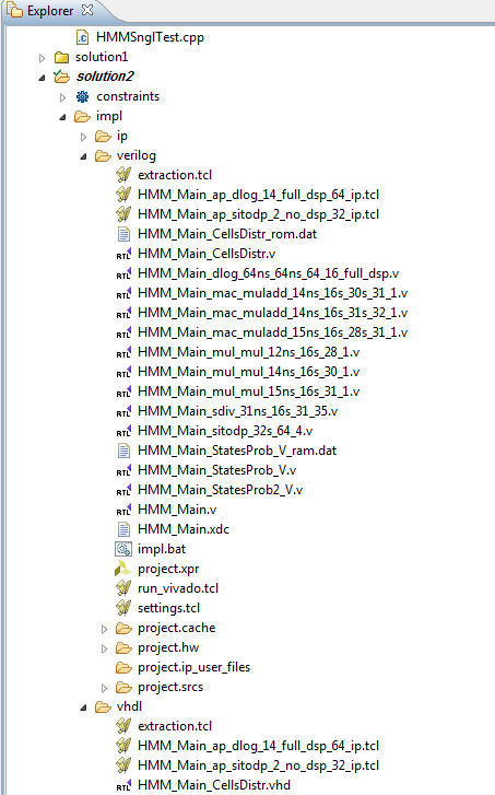
You can also see that RTL Export did create new project directories for your prototype in VHDL or Verilog languages according to what you have selected in Export RTL Dialog Box.
Having these files allows you to use your design in any vhdl or verilog
development platform. These source files are never used by Vivado.
Creating Embedded System with DMA Access
In this section we will create the digital system to which our prototype will be connected.
We will create a simple Zynq processor SoC (System on Chip) project and add components necessary to access system memory using DMA (Direct Memory Access).
The advantage of using DMA is that, the processor is not used directly to transfer the data between the prototype and system memory.
With DMA, data are exchanged directly between memory controller (inside the Zynq chip) and our prototype.
Open Vivado and click on New Project
At New Project Wizard, select project name and project directory. Project directory must be different than Vivado HLS Project directory. Click Next
Select a Zynq device or board. You are free to select any part of the Zynq family. Click Next then Finish
To be able to insert our prototype inside Vivado project, we need to insert a reference to our IP.
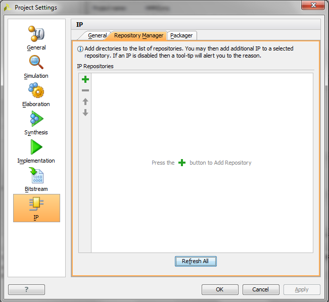
Click on Project Settings
Click on IP and click to select Repository Manager.
CLick on the + button.
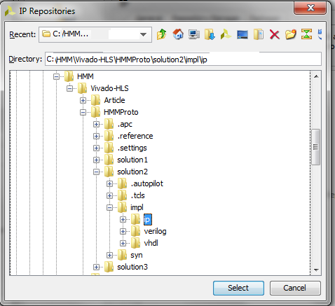
Navigate to HMMProto/solution2/imp/ip directory and click Ok. You should receive a confirmation message that 1 IP was found.
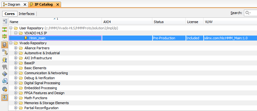
To examine available IPs, you can click on IP Catalog to open IP Catalog and check that our prototype is well defined.
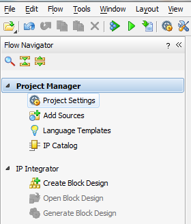
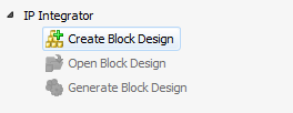
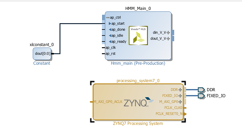
Click on Create Block Design
In the design_1 Diagram, right click and select Add IP...
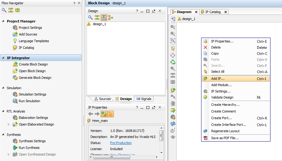
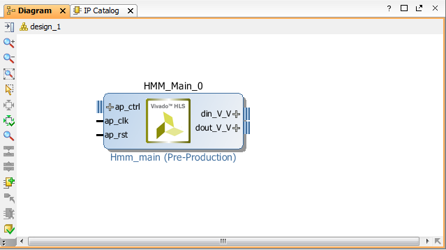
Select HMM_main and double click on it to insert it in the diagram. If Vivado asks you if you want to insert it or to customize it, select insert it.
Right click inside the diagram and select Add IP.... Search for Constant IP and double click it to insert it in the diagram. Connect the constant to the ap_start pin
Select Add IP again and search for Zynq system. Double click it to insert it inside the diagram.

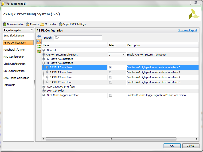
Double click on the Zynq box to configure it. Select PS-PL Tab and enable S AXIS HP0 interface.
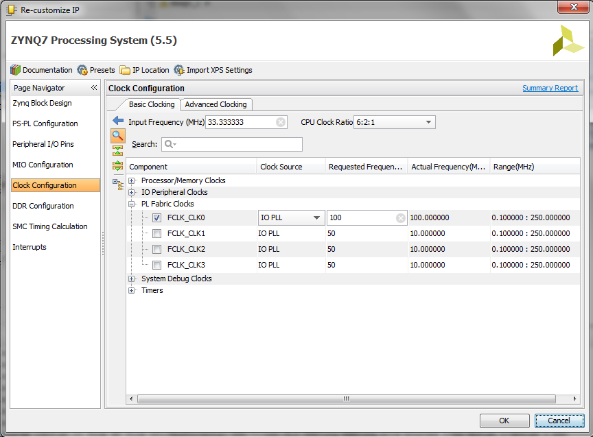
Select Clock Configuration and enable the FLCK_CLK0. Click Ok to finish customization.
Click on Run Block Automation, select All Automations and click Ok. This will automatically create block level interface pins for processor connection to the external DDR memory ports.
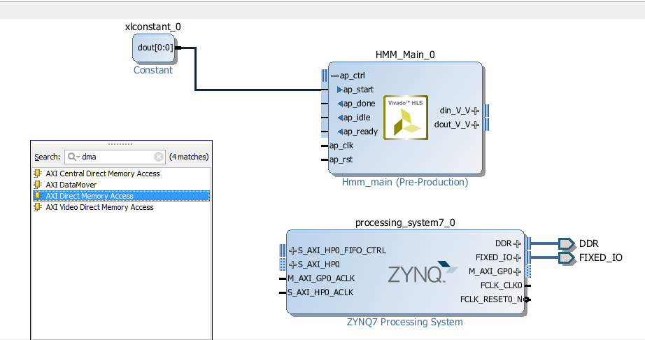
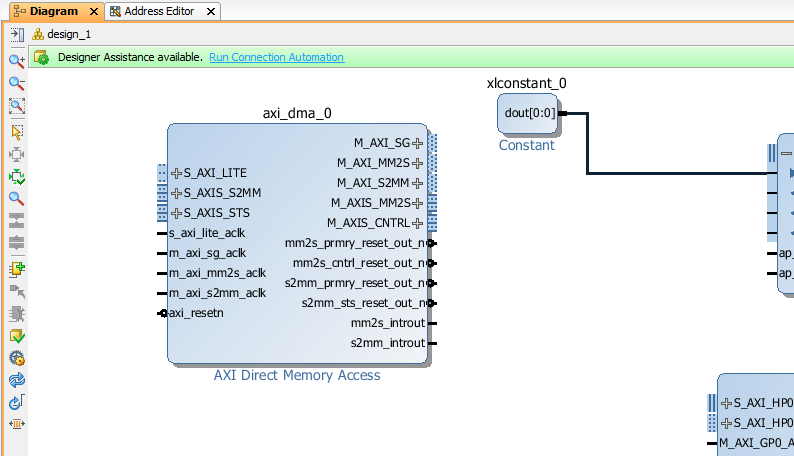
If DMA controller was inserted automatically by Vivado, then go to the next step. Otherwise, right click in the diagram and select Add IP.... Search for DMA and double click on AXI Direct Memory Access
Click on Run Block Automation, select All Automations and click Ok. This will automatically create AXI Interconnect components necessary for connecting the processor to DMA controller and the DMA controller to the HP0 ports.
If Run Block Automation is available again then click it and select All Automations and click Ok.
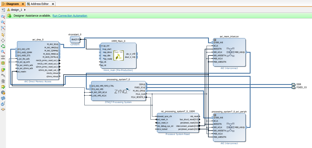
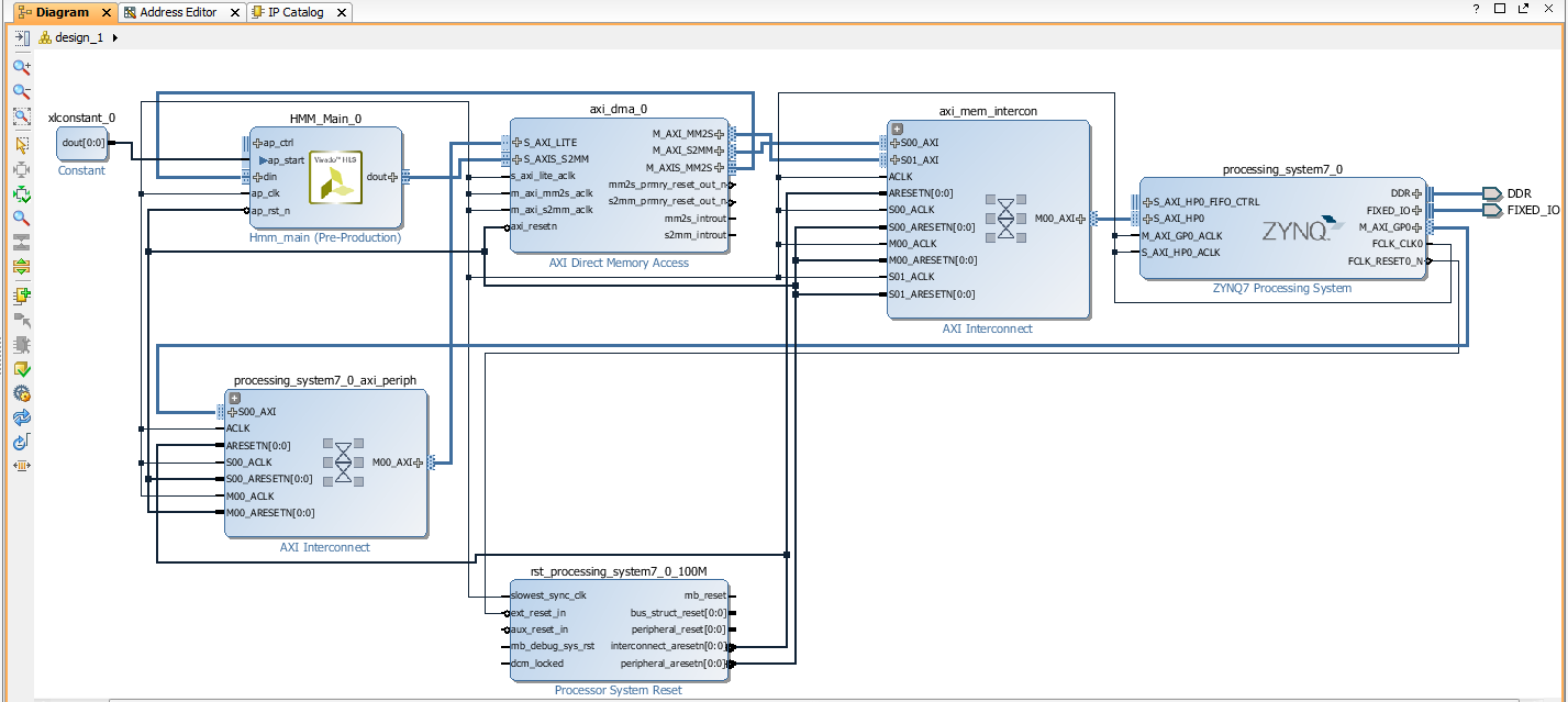
Connect prototype input pins to the DMA output as in the diagram below.
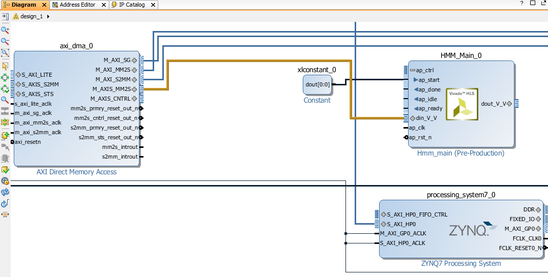
Also, Connect our prototype output pins to the DMA input as in the diagram below.
Your diagram should looks like the diagram bellow.
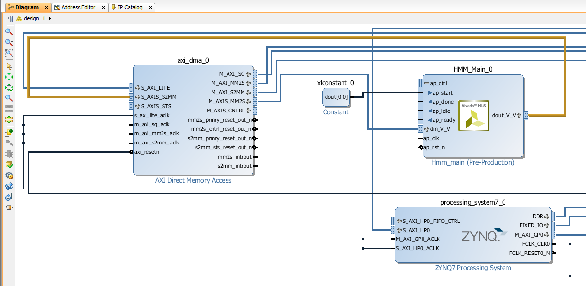
Connect peripheral_arestn to the HMM_Main_0's ap_rst_n pin.
Connect FCLK_CLK0 to HMM_Main_0's ap_clk pin.
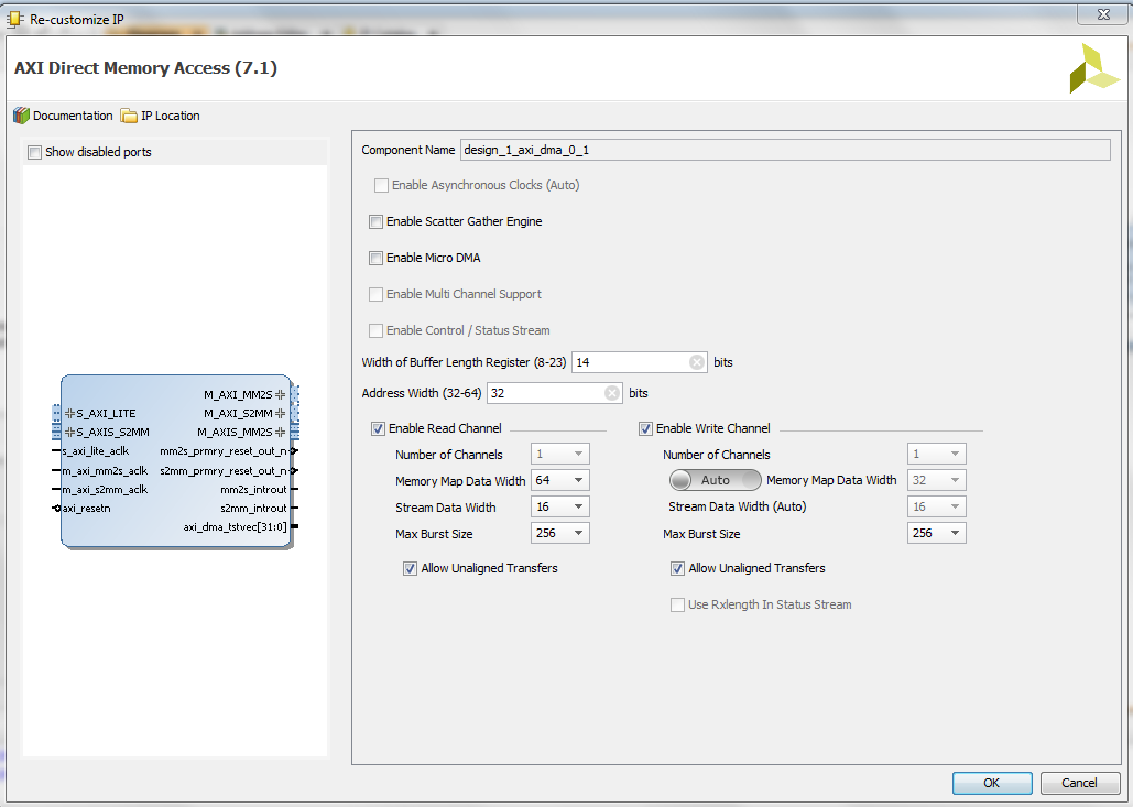
Double click on DMA block and disable Enable Scatter Gather Engine then click Ok
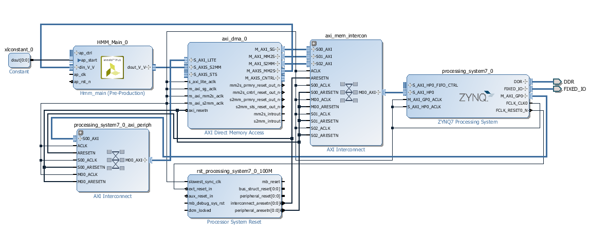
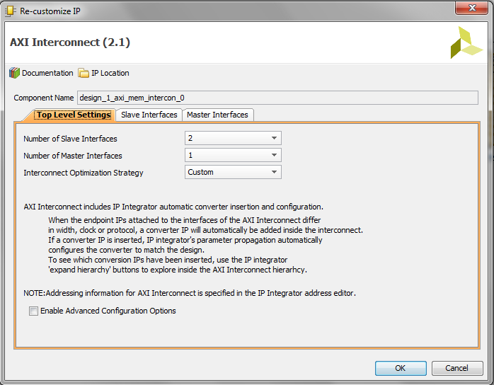
Double click on axi_mem_intercon and select 2 for the number of slave interfaces then click Ok
You may have to reconnect DMA to axi_mem_intercon to obtain the connections as in the diagram below.
To make sure that you have completed all the steps correctly, it is important to select menu item Tools->Validate Design.
This will notify you about any missing connections.
Now that we have finished block design, we are ready to generate the system. From Vivado perspective, our block design is just a block design and it is still considered as external to the project.
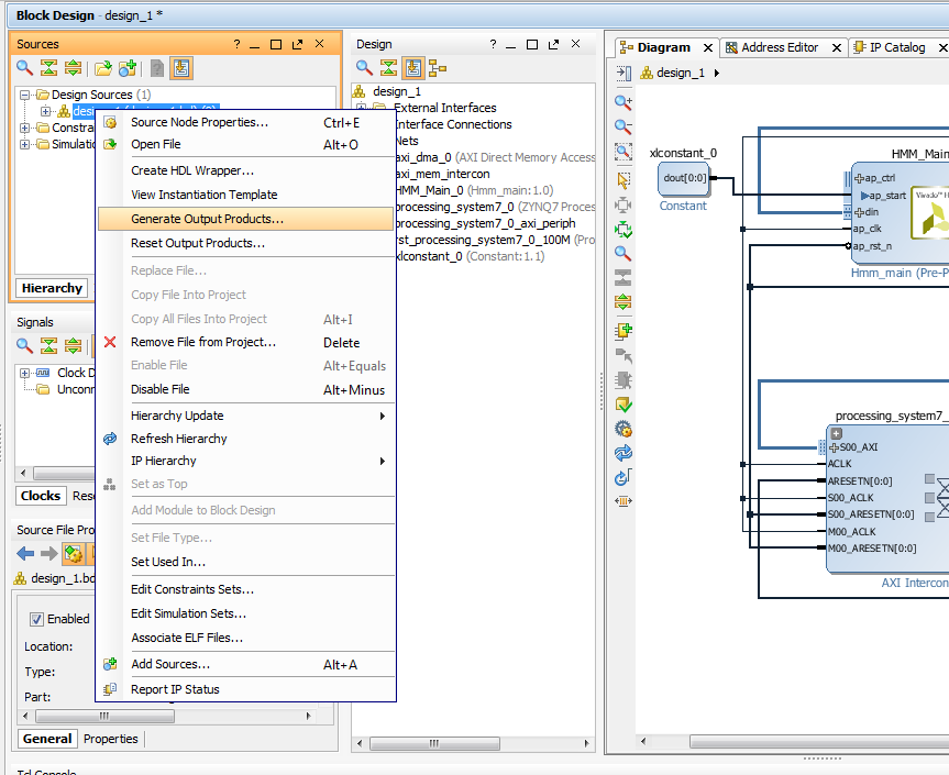
To insert the block diagram into project source, right click on design_1 in sources window, and select Generate Output Products
Again, right click on design_1 in sources window, and select Create HDL Wrapper....
This will generate the top level VHDL, or Verilog, source file that contains all the components defined in the Block Diagram.
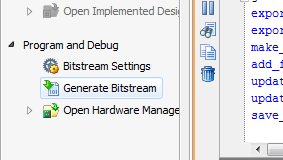
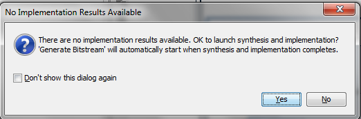
Click on Generate Bitstream
Select Yes to start the synthesis and implementation process.
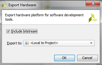
After that the implementation is completed, we are ready to export our design to SDK for software development. For that, select menu item
File->Export->Export Hardware.... At the prompt box select include bitstream and click Ok.
Select menu item File->Launch SDK to open Software Development Kit. At
this point, it is important to understand that vivado did generate automatically
all necessary device drivers and configuration paramters for all components in our design.
When the SDK is opened for the first time, it will displays the memory map for the hardware system
file system.hdf.
This file contains address map necessary to communicate between different system components. Because our prototype uses
AXi4-Stream interface for DMA access we do not need to send direct commands to our prototype.
Instead, we can use provided DMA functions to send and receive data from the prototype.
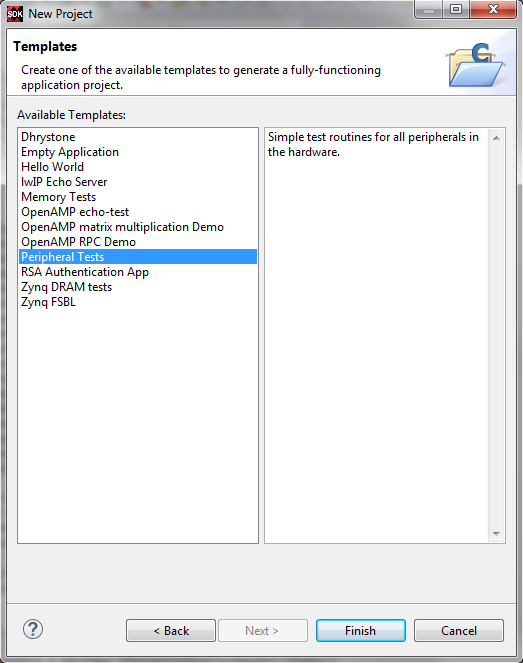
To start developing the software to use the prototype, we have to create a new application based on the hardware design we made previously.
Select menu item File->New->Application Project. Enter project name, select the OS in case you want to run Linux, or other
OS, on the embedded system.
Select design_1_wrapper_hw_platform_0 as the hardware platform and click Next.
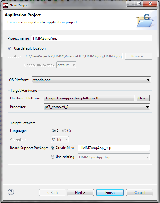
Select Peripheral Tests then click Finish
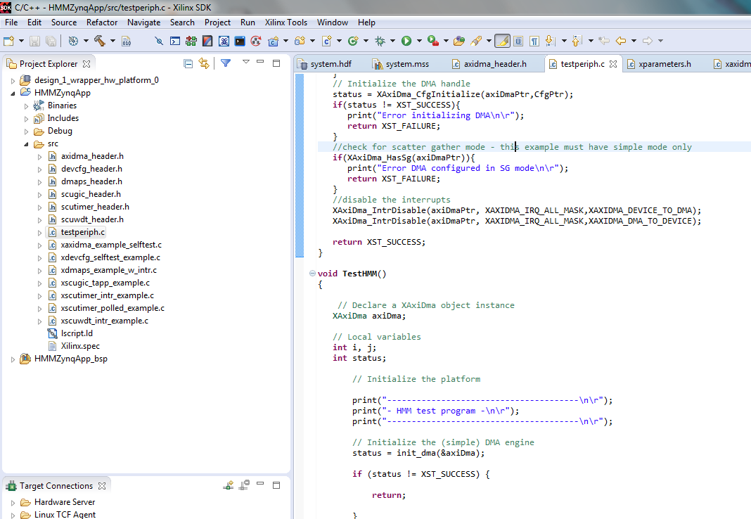
Open the file testperiph.c, delete all the text and pass the text in testperiph.c provided by this tutorial.
You can examine the code in TestHMM function and see that DMA operations are performed by simple calls to Xilinx DMA access functions.
Finally, you can build your project and download it to your FPGA for debuging.
Conclusion
In this tutorial we did not try to realize optimal solution. Further development is necessary to examine the capability of Vivado HLS to provide such solution.
Still, in all cases, as we have demonstrated, Vivado HLS represents a powerful tool for rapid prototype development and excellent compromise between solution performance and development time.